The aim of this project is to develop and automize novel laser cutting processes suitable for the processing of complex CMOS wafers including structured heterogeneous materials.
ALPHONSE
Partner Call open until: June 30, 2025
Project Start: Q3 2025
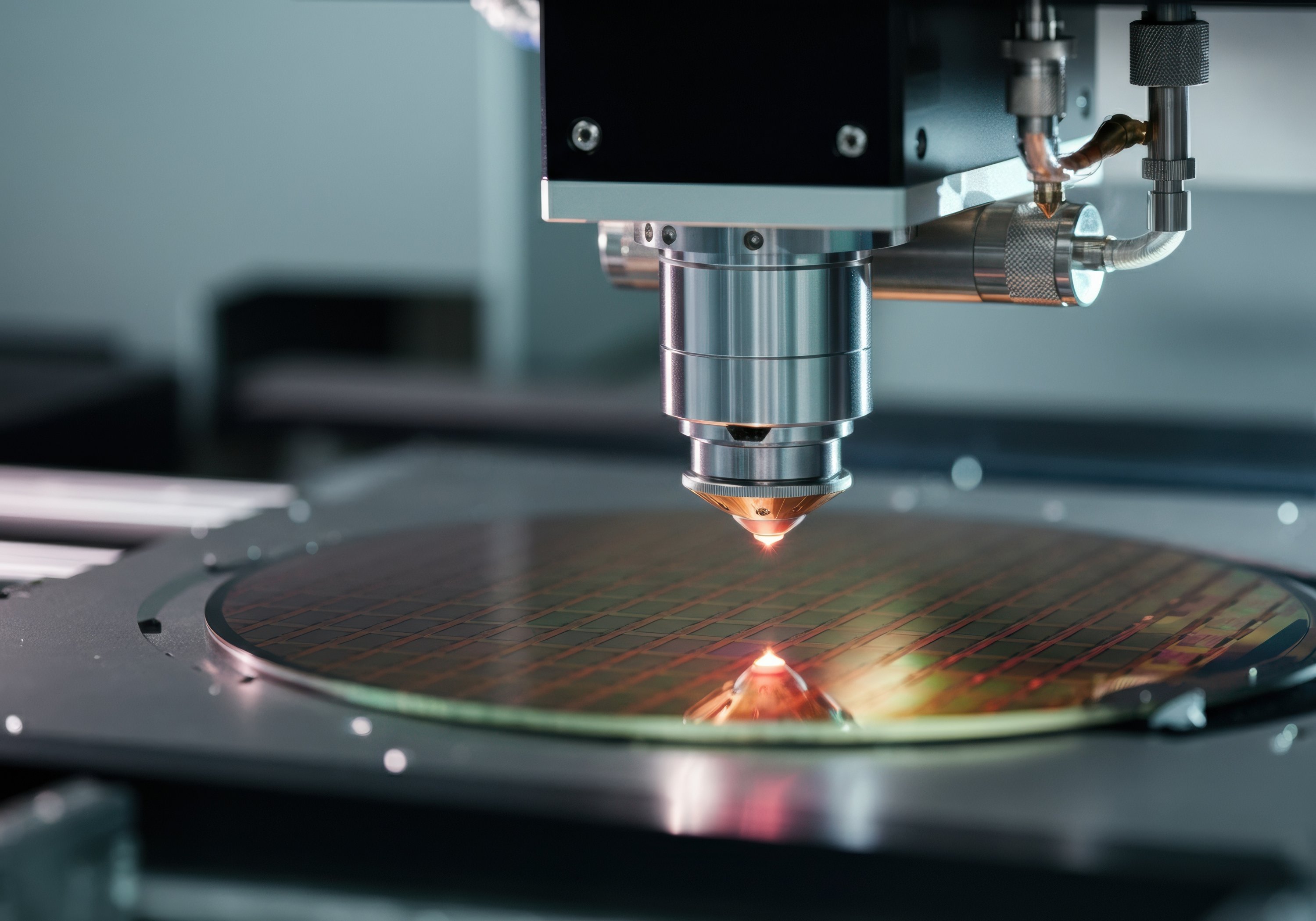
The project aims to develop novel approaches for laser processing in the field of semiconductors. Among the main focuses of the project is a deeper understanding and investigation of the processing of heterogeneous layers, which requires the development of ad-hoc strategies. The main challenges are:
- Control of the shape of the processed area in presence of materials with different absorption and thermal properties.
- Processing of 3D heterogeneous materials
- Implementation of a semi-automized process to simplify the handling of large number of samples
Expected results
- Improvement of laser processing technologies
- Innovative approach for highly efficient processing of heterogeneous 3D structures, especially those based on CMOS materials