A measurement system is developed to allow for quantitative electric field induced second harmonic generation measurements. It will be applied to various semiconductor multilayer samples to infer the interface trap density at those samples and compare them to existing methods.
QUANTITATIVE ELECTRIC FIELD INDUCED SECOND HARMONICS
Partner Call open until: 31.03.2026
Project Start: April 2026
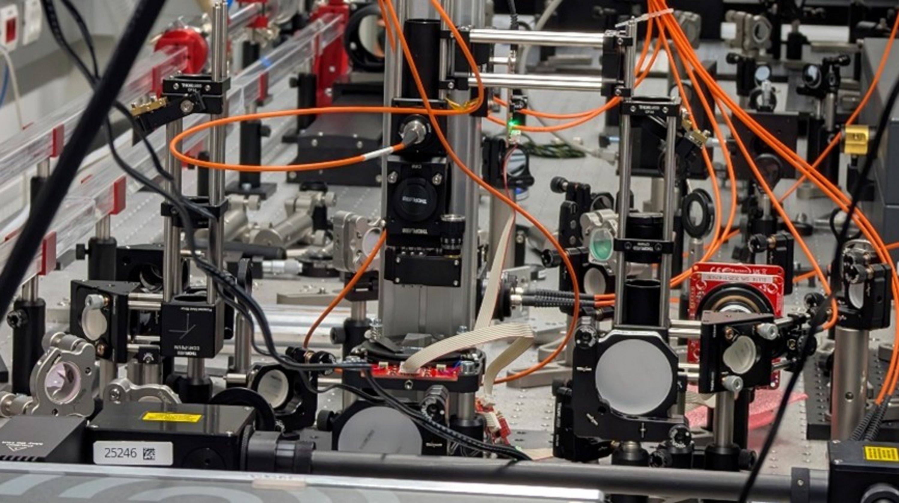
Interface defects are ubiquitous in semiconductor devices and dominate device reliability and performance. During process development, a remote contact free method to is highly attractive to assess interface quality. The electric field of trapped charges breaks the crystals symmetry and enhances second harmonic generation. Based on this mechanism, a quantitative, laser-based measurement system will be developed to allow contact free measurement of the defect density at semiconductor-dielectric interfaces.
Expected results
- Lab based measurement system
- Quantitative, contact free measurements of interface defects of selected samples